Google is reportedly advancing its development of a new generation of artificial intelligence (AI) chips, with South Korean technology giant Samsung emerging as a potential key manufacturing partner. Sources indicate that Samsung is in discussions with Google to produce critical components for these upcoming AI accelerators, signaling a significant collaboration in the highly competitive semiconductor landscape. This move could mark a pivotal moment for Samsung’s foundry business and further solidify Google’s commitment to in-house AI hardware development.
The "Icefish" TPU: A Leap in AI Acceleration
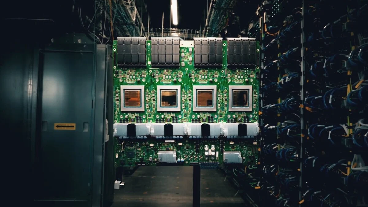
The chip in question is understood to be the tenth generation of Google’s Tensor Processing Unit (TPU), codenamed "Icefish." TPUs are custom-designed ASICs (Application-Specific Integrated Circuits) developed by Google to accelerate machine learning and AI workloads. They are instrumental in powering Google’s vast array of AI-driven services, from natural language processing and image recognition to the increasingly sophisticated generative AI models that are reshaping the digital world. The development of more powerful and efficient TPUs is crucial for Google to maintain its competitive edge in AI research and deployment.
According to recent reports from The Information, Samsung is expected to manufacture the interconnect components that link the main processing chip with memory modules. This crucial task is slated to utilize Samsung’s advanced 2nm fabrication process. The primary computation chip itself, however, is reportedly still being manufactured by Taiwan Semiconductor Manufacturing Company (TSMC), a long-standing and dominant player in advanced chip manufacturing. This division of labor highlights the intricate supply chains and specialized expertise required for cutting-edge semiconductor production.
A Collaborative Endeavor in Chip Design
Further underscoring the collaborative nature of this development, Google is reportedly partnering with MediaTek in the design phase of the new TPU. This collaboration with a prominent fabless semiconductor company like MediaTek suggests a strategic approach by Google to leverage external design expertise and accelerate the complex design process of its next-generation AI hardware. The involvement of multiple industry leaders—Google for design and core architecture, MediaTek for design collaboration, TSMC for the main chip fabrication, and Samsung for component manufacturing—illustrates the escalating complexity and the need for a broad ecosystem of partners in the modern semiconductor industry.
Historically, TSMC has been the primary manufacturer for almost all of Google’s TPUs, dating back to the earliest generations. This includes the recently unveiled TPU v7, codenamed "Ironwood," which utilizes TSMC’s 3nm fabrication process and is expected to be deployed in 2025. The roadmap suggests a continued reliance on TSMC for subsequent generations, with the eighth and ninth generations of TPUs also reportedly set to employ TSMC’s 2nm process. The "Icefish" generation, however, appears to be a significant shift, with the main computation chip potentially moving to an even more advanced 1.4nm process, while the memory I/O components will leverage Samsung Foundry’s 2nm technology. This strategic diversification of manufacturing partners indicates Google’s intent to optimize for specific technological advantages and potentially mitigate risks associated with over-reliance on a single supplier.
Samsung’s Foundry Ambitions and the 2nm Advantage
For Samsung, securing a manufacturing contract from Google for its cutting-edge AI chips would represent a significant victory. The company’s foundry business has faced considerable challenges in attracting major clients in recent years, particularly in the highly competitive arena dominated by TSMC. The ability to successfully produce components using its 2nm fabrication technology for a high-profile client like Google would not only bolster Samsung’s reputation but also serve as a powerful testament to its manufacturing capabilities.

The 2nm fabrication process represents a critical advancement in semiconductor technology, offering enhanced performance and power efficiency compared to previous generations. This technology is essential for the increasingly demanding applications of AI, where faster processing and lower energy consumption are paramount. By demonstrating its prowess in this advanced node, Samsung aims to attract more high-value customers and solidify its position as a leading foundry provider.
The Evolving Landscape of AI Hardware Manufacturing
The trend of major technology companies developing and manufacturing their own custom AI chips is a defining characteristic of the current technological era. Companies like Google, Amazon, Microsoft, and Apple are increasingly investing in in-house silicon design to gain greater control over performance, optimize for specific workloads, and differentiate their products and services. This approach allows them to tailor hardware precisely to their software needs, leading to significant improvements in efficiency and capability.
The involvement of multiple foundries in the production of a single advanced chip also reflects the growing specialization within the semiconductor industry. TSMC, with its established leadership in leading-edge process nodes, remains a crucial partner for many chip designers. However, companies like Samsung are rapidly closing the gap, investing heavily in research and development to offer competitive manufacturing solutions. The potential collaboration between Google and Samsung underscores a broader industry shift towards a more distributed and specialized manufacturing ecosystem.
Strategic Implications and Future Outlook
The implications of this collaboration are far-reaching. For Google, it signifies a continued commitment to pushing the boundaries of AI hardware, enabling them to accelerate their research and development in areas such as large language models, computer vision, and autonomous systems. The ability to leverage Samsung’s manufacturing expertise for specific components could lead to more cost-effective and scalable production of their advanced TPUs.
For Samsung, this partnership is a much-needed boost to its foundry division. It demonstrates their ability to compete at the highest levels of advanced semiconductor manufacturing and could pave the way for future collaborations with other major tech companies seeking cutting-edge fabrication capabilities. The success of this venture could significantly impact the competitive dynamics within the foundry market, potentially challenging TSMC’s long-held dominance.
The timeline for the "Icefish" TPU’s deployment remains speculative, but given the typical development cycles for such advanced chips, it is likely to be several years away. However, the early reports of this collaboration highlight the rapid pace of innovation in the AI hardware space and the strategic importance of securing advanced manufacturing partnerships. As AI continues to permeate every aspect of technology and business, the race to develop and produce the most powerful and efficient AI chips will only intensify, with collaborations like this playing a crucial role in shaping the future of the industry. The intricate dance between chip design, manufacturing, and technological advancement is set to redefine the capabilities of artificial intelligence for years to come.