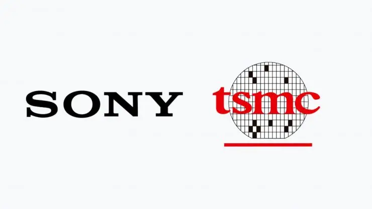
Sony, a titan in the imaging sensor market, has announced a significant strategic partnership with Taiwan Semiconductor Manufacturing Company (TSMC), the world’s leading contract chip manufacturer, to co-develop next-generation camera sensors. This ambitious joint venture will be established at a new Sony facility in Koshi, Kumamoto Prefecture, Japan. Under this groundbreaking collaboration, Sony will spearhead the technological development and design of these advanced image sensors, while TSMC will leverage its unparalleled expertise in semiconductor manufacturing to produce the intricate chips. This move signals a pivotal shift in Sony’s manufacturing strategy, aimed at reducing its reliance on in-house production and embracing a more collaborative, "fab-light" model.
The announcement comes at a time when the demand for increasingly sophisticated camera sensors is soaring, driven by the relentless evolution of smartphones, professional cameras, and other imaging devices. Sony’s dominance in this sector, supplying sensors to a vast array of global brands, positions this partnership as a critical development for the future of imaging technology.
A Strategic Shift Towards a "Fab-Light" Model
Sony CEO Hiroki Totoki has explicitly described this initiative as the commencement of the company’s "fab-light" strategy. This approach signifies a deliberate pivot, allowing Sony to concentrate its resources and innovation efforts on the conceptualization, research, and development of cutting-edge imaging technologies and intellectual property (IP). By outsourcing the complex and capital-intensive manufacturing processes to specialists like TSMC, Sony aims to optimize its operational efficiency and accelerate the pace of innovation. This strategic reorientation has been subtly unfolding over time, with Sony gradually scaling back its direct involvement in certain other manufacturing lines, signaling a broader trend within the company’s operational philosophy.
The decision to partner with TSMC is particularly noteworthy given the sheer complexity and escalating demands of modern camera sensor design. The integration of advanced technologies, such as stacked sensor architectures and sophisticated on-chip processing, requires manufacturing capabilities that are at the absolute forefront of the semiconductor industry. TSMC’s established prowess in producing some of the world’s most advanced logic chips makes it an ideal partner for Sony, ensuring that its next-generation sensor designs can be realized with the precision and scale required to remain competitive in a rapidly evolving global market.
The Global Reach of Sony’s Imaging Sensors
Sony’s position as a dominant force in the imaging sensor market is underscored by the widespread adoption of its technology across a diverse spectrum of consumer and professional devices. In the smartphone arena, Sony’s sensors are integral to the camera systems of flagship models from leading manufacturers, including Apple’s iPhone, Google’s Pixel series, and OnePlus devices. This widespread integration is a testament to the quality, performance, and reliability that Sony sensors consistently deliver.
Beyond the mobile space, Sony’s influence extends deeply into the professional photography and videography industries. Renowned camera manufacturers such as Nikon, Fujifilm, and Leica have incorporated Sony sensors into their high-end digital cameras, recognizing their superior image capture capabilities. Furthermore, the burgeoning drone and cinematic camera markets also rely heavily on Sony’s imaging prowess, with companies like DJI and Blackmagic Design utilizing their sensors for their advanced aerial and professional filmmaking equipment. This broad market penetration highlights the critical role Sony plays in shaping the visual landscape across numerous industries. The success of this new joint venture with TSMC could further solidify Sony’s already formidable position as a key architect of global imaging innovation.
A Timeline of Technological Advancement and Collaboration
While the specifics of the joint venture’s timeline are still emerging, the genesis of this collaboration can be traced back to the increasing complexity of sensor technology and the evolving dynamics of the semiconductor supply chain.
Early 2010s: Sony begins to significantly invest in and develop advanced sensor technologies, including backside-illuminated (BSI) sensors and early iterations of stacked sensor designs. This period marks a significant leap in sensor performance, enabling better low-light capabilities and faster readout speeds.
Mid-2010s: The adoption of Sony sensors by major smartphone manufacturers accelerates, solidifying their dominance in the mobile imaging market. The demand for higher resolutions, improved dynamic range, and advanced features like faster autofocus becomes paramount.
Late 2010s – Early 2020s: The trend towards increasingly complex sensor architectures, including the widespread adoption of stacked CMOS sensor technology, gains momentum. This technology allows for greater functionality and processing power to be integrated directly onto the sensor, leading to significant performance improvements. However, this also necessitates more sophisticated manufacturing processes. The global semiconductor supply chain faces increasing strain due to escalating demand and geopolitical factors, prompting companies to re-evaluate their manufacturing strategies and forge strategic alliances.

2023-2024 (Inferred): Discussions and negotiations between Sony and TSMC likely intensify. Sony recognizes the need for TSMC’s advanced manufacturing capabilities to realize its next-generation sensor designs, particularly those incorporating cutting-edge lithography and fabrication techniques. TSMC, in turn, sees the strategic value of partnering with a leading sensor designer like Sony, securing a long-term demand for its advanced manufacturing services in a critical growth sector.
Announcement (Current): The formal announcement of the joint venture is made, outlining the establishment of a new facility in Koshi, Japan, and the division of responsibilities between Sony’s design expertise and TSMC’s manufacturing prowess. This marks a significant milestone in their strategic collaboration.
Future Development: The joint venture will focus on the research, development, and manufacturing of advanced camera sensors, likely incorporating technologies such as AI-powered image processing, enhanced spectral sensitivity, and further miniaturization for next-generation devices.
Supporting Data and Industry Context
The global image sensor market is a substantial and growing sector. Projections from market research firms consistently indicate a robust upward trend, driven by the proliferation of smart devices, automotive imaging systems, and advanced surveillance technologies, in addition to the traditional photography and smartphone markets.
- Market Size: The global image sensor market was valued at approximately USD 20 billion in 2022 and is projected to grow at a Compound Annual Growth Rate (CAGR) of over 7% in the coming years, potentially reaching over USD 30 billion by 2028.
- Dominance of CMOS: Complementary Metal-Oxide-Semiconductor (CMOS) sensors, which Sony primarily produces, currently dominate the market due to their lower power consumption, higher integration capabilities, and faster read speeds compared to older CCD technology.
- Advancements in Stacked Sensors: Stacked CMOS sensor technology, which separates the pixel layer from the circuit layer, has been a key innovation. This allows for more sophisticated signal processing to be integrated directly onto the sensor, leading to enhanced speed, lower noise, and improved image quality. Sony has been a leader in this domain.
- Automotive Imaging: The automotive sector is a rapidly growing segment for image sensors, with increasing demand for cameras used in Advanced Driver-Assistance Systems (ADAS), autonomous driving, and in-cabin monitoring. This sector requires highly reliable and robust sensors capable of performing in challenging environmental conditions.
- The Role of Foundries: TSMC’s dominance in the semiconductor foundry market is undeniable. The company manufactures chips for a vast array of fabless semiconductor companies, including Apple, NVIDIA, and AMD, and is renowned for its cutting-edge manufacturing processes, including advanced FinFET and potentially future Gate-All-Around (GAA) transistor technologies.
Official Statements and Industry Reactions (Inferred)
While direct quotes from TSMC leadership regarding this specific joint venture may not yet be publicly available, their general stance on strategic partnerships and their commitment to advanced manufacturing is well-documented.
Sony’s Perspective: As articulated by CEO Hiroki Totoki, the "fab-light" strategy emphasizes a focus on core competencies in R&D and IP development. This partnership allows Sony to harness TSMC’s manufacturing excellence without the massive capital expenditure and operational overhead associated with building and maintaining its own state-of-the-art fabrication facilities. This is likely seen as a move to enhance agility and competitiveness.
TSMC’s Perspective (Inferred): For TSMC, this partnership represents a significant opportunity to solidify its position as the go-to manufacturer for advanced imaging sensors. By collaborating with a leading sensor designer like Sony, TSMC gains deeper insights into the specific technological requirements and future trends in the imaging sector, potentially driving further innovation in their own manufacturing processes. This also aligns with TSMC’s strategy of diversifying its customer base and strengthening its presence in high-growth markets.
Industry Analyst Reactions (Inferred): Industry analysts are likely to view this collaboration as a logical and potentially highly impactful development. They may highlight:
- Synergistic Strengths: The clear alignment of Sony’s design innovation with TSMC’s manufacturing mastery.
- Competitive Advantage: The potential for this partnership to produce sensors that further solidify Sony’s market leadership and push the boundaries of imaging technology.
- Supply Chain Resilience: The establishment of a dedicated joint venture facility in Japan could also be seen as a move to enhance supply chain resilience and potentially address geopolitical concerns by diversifying manufacturing locations.
Broader Impact and Implications
The implications of this Sony-TSMC collaboration extend far beyond the two participating companies, potentially reshaping the landscape of digital imaging and the broader semiconductor industry.
- Accelerated Innovation: By combining Sony’s R&D prowess with TSMC’s manufacturing capabilities, the pace of innovation in camera sensor technology is likely to accelerate. This could lead to faster development cycles for new features and performance enhancements, benefiting consumers and professionals alike.
- Setting New Industry Standards: The sensors developed through this joint venture could set new benchmarks for image quality, speed, power efficiency, and advanced functionalities, influencing the direction of sensor development across the industry.
- Impact on Competitors: Other sensor manufacturers may feel increased pressure to form similar strategic alliances or significantly invest in their own advanced manufacturing capabilities to remain competitive.
- Geopolitical Considerations: The establishment of a high-tech manufacturing facility in Japan, a country with strong technological infrastructure and a stable political environment, could be seen as a strategic move to mitigate some of the risks associated with global supply chain disruptions. This aligns with broader trends of regionalizing critical manufacturing capabilities.
- Evolution of "Fab-Light" Models: Sony’s success with this "fab-light" strategy in the sensor domain could serve as a model for other technology companies looking to optimize their R&D and manufacturing operations. It highlights a growing trend where companies focus on their core intellectual strengths while leveraging external expertise for specialized production.
- Future of Imaging: The joint venture is poised to play a crucial role in enabling future advancements in areas such as computational photography, augmented reality (AR), virtual reality (VR), and automotive sensing, all of which rely on increasingly sophisticated imaging sensors.
In conclusion, Sony’s strategic alliance with TSMC for the development and manufacturing of next-generation camera sensors represents a significant milestone. It underscores a forward-thinking approach to innovation and production, aiming to leverage specialized expertise to maintain a competitive edge in a rapidly evolving technological landscape. The success of this joint venture could have profound and lasting effects on the future of digital imaging and the global semiconductor industry.