
Shanghai, China – In a significant announcement at the IEEE International Symposium on Circuits and Systems (ISCAS) held in Shanghai, Chinese technology giant Huawei has introduced a groundbreaking concept named the Tau (Ï„) Scaling Law, positioning it as a potential successor to the venerable Moore’s Law. Huawei’s ambitious projection suggests that this novel approach could enable the company to achieve chip performance equivalent to 1.4nm manufacturing processes by the year 2031.
For decades, Moore’s Law, an observation by Intel co-founder Gordon Moore, has served as a foundational benchmark for the semiconductor industry. It posited that the number of transistors on an integrated circuit would double approximately every two years, leading to exponential increases in computing power and corresponding decreases in size and cost. However, the relentless pursuit of shrinking transistor dimensions has encountered formidable physical and economic barriers in recent years. Manufacturing costs have soared, design complexity has become astronomically high, and the rate of performance improvement has begun to plateau, prompting the industry to seek new paradigms for advancement.
The Genesis of Tau Scaling Law
Huawei’s Tau Scaling Law represents a paradigm shift, moving the focus from purely physical miniaturization to optimizing the efficiency of signal propagation within a chip. Instead of solely concentrating on making transistors smaller, this new concept prioritizes how quickly and efficiently data can traverse the processor. This emphasis on signal latency and propagation time aims to unlock new avenues for performance enhancement, even as traditional scaling faces limitations.
The company has asserted that the Tau Scaling Law is not merely theoretical. Huawei claims to have already achieved mass production of 381 chips based on this principle, catering to diverse industrial applications. While the term "1.4nm equivalent" may not directly translate to Huawei utilizing a 1.4nm manufacturing node in the traditional sense, as defined by leading foundries like TSMC or Samsung, it likely signifies the achievement of performance and transistor density comparable to that benchmark through a combination of advanced architectural design and internal optimization strategies. This distinction is crucial, as it suggests Huawei is leveraging innovative design methodologies rather than solely relying on access to the most cutting-edge fabrication facilities.
A Historical Perspective on Semiconductor Advancement
The journey of semiconductor technology has been a testament to human ingenuity. Following the invention of the transistor in 1947, the integrated circuit in 1958, and the microprocessor in 1971, the industry entered an era of unprecedented growth. Moore’s Law became the guiding principle, driving innovation across consumer electronics, telecommunications, and computing. Early on, the scaling of transistors allowed for more powerful and compact devices, from room-sized computers to the smartphones we carry today.
However, as transistors approached atomic scales, quantum mechanical effects began to pose challenges. Tunneling, leakage currents, and heat dissipation became significant hurdles. The economic viability of developing and operating fabrication plants capable of producing these minuscule components also became a major concern. The cost of building a leading-edge semiconductor fabrication facility has escalated into the tens of billions of dollars, making it an exclusive domain for a handful of global players. This escalating cost and complexity have led many analysts to predict the eventual slowdown or end of Moore’s Law as we’ve known it.
Huawei’s Response to Industry Challenges
Huawei’s introduction of the Tau Scaling Law can be viewed as a strategic response to these industry-wide challenges, particularly in the context of its own geopolitical and technological constraints. Facing restrictions on its access to advanced chip manufacturing technologies from Western suppliers, Huawei has been compelled to explore alternative pathways for technological advancement. The Tau Scaling Law and its accompanying architectural innovations appear to be central to this strategy, allowing the company to enhance chip performance and efficiency through clever design and process integration, rather than solely relying on the most advanced foundry nodes.
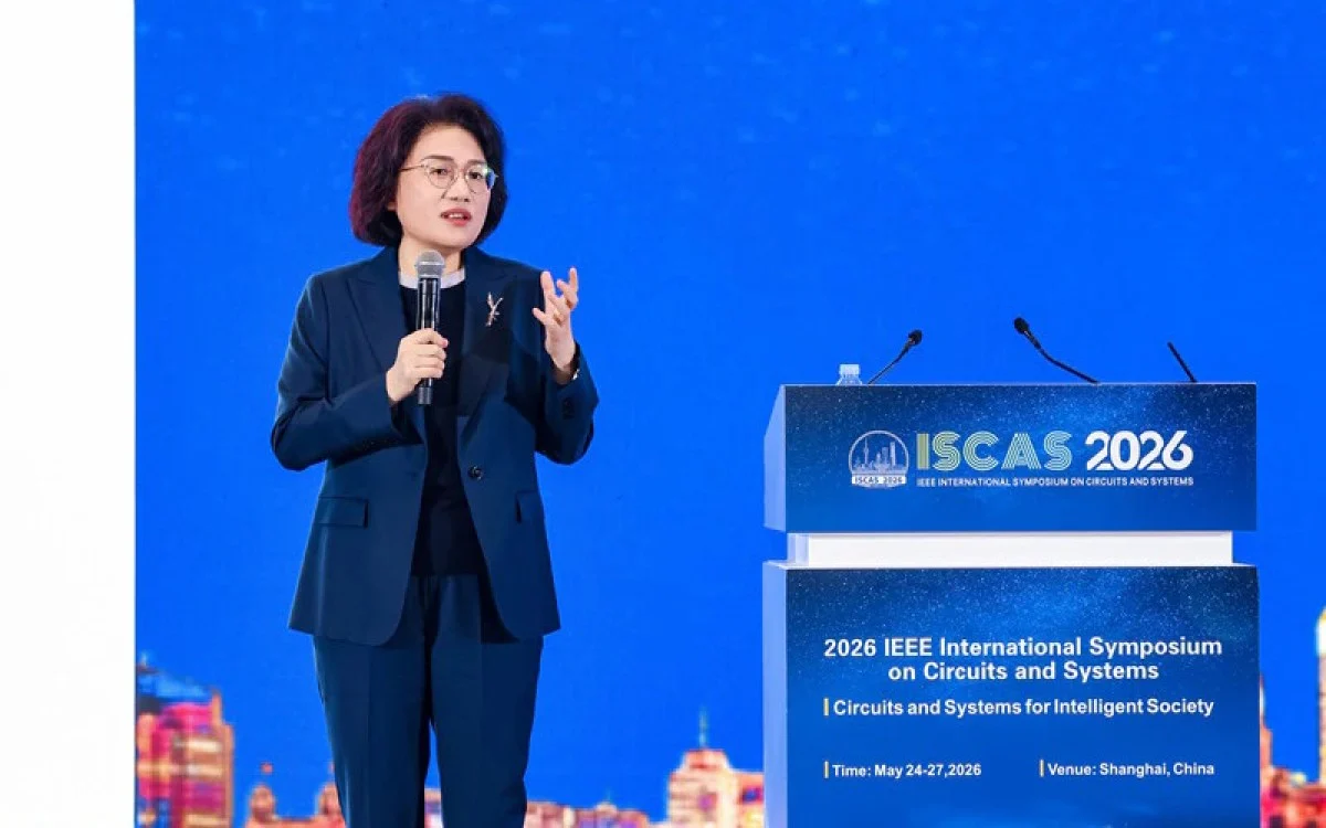
The company’s presentation at ISCAS, a prominent international forum for circuit and systems research, underscores the academic and scientific rigor behind their claims. ISCAS typically brings together leading researchers, engineers, and academics to discuss the latest advancements in electronics, signal processing, and related fields. Huawei’s participation and announcement at such a venue signal their intent to present their work on a global stage and to engage with the broader scientific community.
The Role of LogicFolding Architecture
Complementing the Tau Scaling Law, Huawei also unveiled a new architecture named LogicFolding. This technology is specifically designed to mitigate signal delay while simultaneously increasing transistor density, thereby reducing the dependency on extreme shrinkage of manufacturing nodes. The potential applications of LogicFolding are broad, extending beyond smartphones to encompass a wide array of electronic systems and processor types. This versatility suggests a long-term vision for how Huawei intends to leverage its R&D capabilities across its product portfolio and potentially for external licensing.
The initial implementation of LogicFolding is slated for the next generation of Kirin processors, expected in 2026. Huawei has stated that these processors will be the first to incorporate this architecture, promising a substantial performance leap compared to their predecessors. This timeline indicates a phased rollout, allowing for further refinement and validation of the technology before wider deployment.
Broader Implications and Industry Analysis
The implications of Huawei’s announcement are far-reaching. If successful, the Tau Scaling Law and LogicFolding architecture could provide a much-needed boost to the semiconductor industry’s innovation cycle, offering a viable alternative to the traditional scaling model. This could democratize access to high-performance computing by potentially lowering the cost and complexity associated with achieving advanced chip capabilities.
For Huawei, this development is crucial for its continued competitiveness in the global market. By demonstrating its ability to innovate and push the boundaries of chip design, the company aims to reaffirm its position as a technology leader, despite external pressures. The focus on internal R&D and novel architectural approaches also highlights a broader trend within the semiconductor industry: the increasing importance of design and software optimization in driving performance, alongside advancements in manufacturing.
Industry analysts will be closely watching Huawei’s progress, particularly the real-world performance of its upcoming Kirin processors. The ability to deliver on the promise of "1.4nm equivalent" performance without necessarily relying on the most advanced manufacturing nodes could set a new precedent for chip development. It also raises questions about the future business models of foundries and the potential for design-centric companies to achieve significant breakthroughs.
While the exact technical details of the Tau Scaling Law and LogicFolding architecture are yet to be fully disclosed, their unveiling at ISCAS represents a significant moment. It signals a potential inflection point in the evolution of semiconductor technology, suggesting that the industry may be entering a new era where innovation is driven by a confluence of architectural ingenuity, efficient signal processing, and optimized design, rather than solely by the shrinking of transistors. The coming years will reveal whether Huawei’s ambitious vision can indeed pave the way for a new era of computing advancement, potentially redefining the landscape of semiconductor development for years to come.